TAPS-6 OUTPUT TRANSFORMERS
This transformer design was developed for the BITS/TAPS
instrument series in 1994-5. The goal was an output
transformer that could provide about 100 W electrical drive
to a 50 Ω
resistive load from our basic switching power amplifier
running on +15V DC.
It was found that two designs were necessary, one for
frequencies up to 700 kHz and another for frequencies above
700 kHz. In all cases, the physical configuration is a 2616
case with PCB mount (2616F1D bobbin in a 2616HD hardware
kit). Primary wires are 20 AWB magnet wire, secondaries are
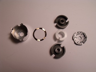
22 AWG. The basic 'kit' of parts is shown below:

LOW
FREQUENCY
The core is a 2616 PL00-3E2A ungapped potcore pair.
A bundle of wires is prepared: 2 primary wires and 8
secondary wires. One end of the group is captured in a vise
and the bundle is twisted together fairly tightly using a
pair of pliers. This bundle is then wrapped tightly around
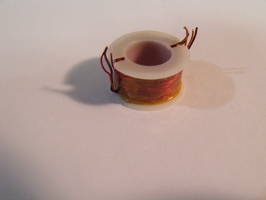
the bobbin 4-1/2 times and wrapped with Kapton tape.

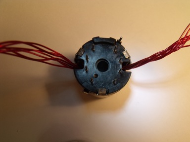
The bobbin and wire bundle is assembled into the potcore
and slipped into the metal can on top of a spring. A
terminal plate is aligned with the tabs on the can and the
tabs forced down to secure the potcore and plate into the
can (fig.below).

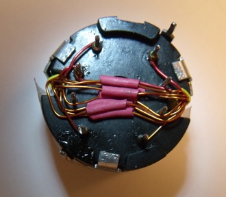
One primary wire from the right-hand (RH) bundle is
soldered to pin 4. The other end of this wire (in the LH
bundle) is found with an ohm-meter and brought across to
pin 3. The other primary wire from the RH bundle is also
soldered to pin 3. The other end of this wire from the LH
bundle is soldered to pin 5. This completes the primary
wiring. One secondary wire from the LH bundle is soldered
to pin 8. The other end (from the RH bundle) is found with
the ohm-meter. This wire is spliced to any wire from the LH
bundle and the splice covered with shrink-tubing. The other
end of this wire (from the RH bundle) is found with the
ohm-meter and it is also spliced to a wire from the LH
bundle. This process continues until only one wire is left
from the RH bundle; this wire is soldered to pin 1.

HIGH
FREQUENCY
This transformer is similar in construction to the
low-frequency transformer, except that the core material is
2616-PL00-3F3. Also, the secondary winding is formed from 5
wires (and the wire bundle is wrapped around the bobbin
3-1/2 times.
DESIGN
The purpose of the output transformer is to efficiently
couple energy from the switching transistors connected to
the +15V power supply to the output load. If we want to
develop, say, 100 W of transmitter power, we will need to
push about 6.7 amps through the switching transistors. On
the load side (we assume 50 ohms here), we need to develop
about 70.7V across the (resistive) load. Thus, we need to
step up the 15V available at the transistors to about 71V
at the load, a step-up ratio of about 4.7:1.
I have used DC voltages in the approximation above. This is
legitimate in this case because the switching amplifier
waveforms are essentially square-waves. The power
dissipated in a resistive load by a square wave is the
square of the peak voltage divided by the resistance (P =
V^2 / R).
Also, I have used the ratio of the output winding to one
primary winding as the step-up ratio. This is a
simplification of a slightly more complicated situation. If
you examine the voltages at the ends of the primary
windings, you will find that it fluctuates between nearly
0V and TWICE the supply voltage. When one transistor is
turned on and current flows in that half of the primary
winding, it induces a voltage in the other winding that
ADDS to the center-tap voltage to produce 2 E volts.
Similarly, when this transistor shuts off and the other
transistor turns on, the voltage on the primary will
reverse and 2 E volts will appear on the opposite winding.
So the turns ratio of the transformer is Vout / 2*Vin if
the whole primary winding is considered. Or, the turns
ratio is Vout / Vin if just one-half of the primary winding
is considered.
I developed an Excel spreadsheet to help me design
transformers. This spreadsheet (see the DOWNLOADS page)
lets you enter the parameters of a particular potcore size
and material and then design a transformer to produce the
power you want from the DC voltage you have available for
your power amplifier. It is specific to a push-pull,
digital amplifier like the ones shown in the SCHEMATICS
sections of the TAPS descriptions. The spreadsheet assumes
that the transistors will have some on-resistance that
prevents the primary end-point voltages from coming quite
to 0V, leading to more realistic estimates of output power.
The spreadsheet also calculates the core flux density for
the given power and frequency for comparison with the
maximum values specified by the manufacturer.


